Taking a Leap Forward in the PE Business
“Technology and Challenges as Seen Through Komori’s 100-Year History” Series (Part 4)
08 July 2026
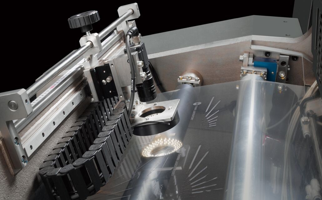
In this series, "Technologies and Challenges Through 100 Years of Komori," we spotlight key technological innovations and business milestones from our century-long history. This article focuses on PE (Printed Electronics), a new business that expands the potential of printing technology into electronic circuit formation.
Komori is renowned for its cutting-edge printing technologies, which represent a sophisticated integration of technology to control flexible objects such as paper, ink, water, and air, coupled with rigid body control technologies including high-precision drive transmission, precision machining, and vibration suppression. These capabilities pose the intriguing question: Can these technologies be effectively applied in other industries? This query marks the commencement of Komori's venture into exploring new fields and applications.
New business utilizing high-precision printing technology
Komori found a significant opportunity to adapt printing technology to fabricate electronic circuits, traditionally produced through photolithography. This complex process involves multiple stages, including sputtering, deposition using CVD, exposure, development, and cleaning on substrates such as glass, ceramic, and PCBs, which are both intricate and environmentally demanding. By harnessing a printing approach that deposits materials precisely where needed, this technology drastically reduces environmental impact manufacturing costs compared to traditional methods that remove and discard excess material. Among various printing techniques, gravure offset printing emerged as the optimal choice for creating fine lines necessary in electronic circuitry. In 2011, Komori launched the PEPIO R20, a roll-to-roll type gravure offset printing press, followed by the introduction of the PEPIO F20, a sheetfed flatbed type, in 2012. These innovations have not only enhanced the precision of line printing but also significantly boosted productivity in the Printed Electronics (PE) business, where they are used to form electronic circuits.
At the 2012 Touch Taiwan exhibition, Komori showcased its commitment to advancing fine-line printing technology through gravure offset printing. During the event, Komori drew significant attention by displaying a metal mesh printing sample. This sample featured a transparent electrode with a narrow line width of 7 μm, using a conductive silver paste intended for use in touch panels. The innovation sparked considerable interest and led to a joint research and development agreement with Taiwan's Industrial Technology Research Institute (ITRI) in January 2013. Further success was demonstrated at the 2013 Touch Taiwan, where Komori unveiled an operational touch panel that had been produced using gravure offset printing with a design rule of L/S=20/20 μm. Komori continued to push the boundaries of this technology, and in October, at FPD International 2013 in Yokohama, introduced an ultra-slim bezel with an even finer L/S=9/9 μm, utilizing roll-to-roll gravure offset technology. This achievement not only garnered the FPD International Award for Excellence but also received extensive media coverage in Japan and Taiwan, resonating strongly with the public.
To successfully commercialize this technology, Komori acquired the former Tokai Group, a company with extensive experience in screen-printing machine for solder resist on PCB substrates. This acquisition not only brought in a company with a strong presence in the electronics industry but also expanded Komori's capabilities beyond manufacturing and selling printing presses. Tokai Group had also been engaged in the plate-making business and operated as a trading company, dealing in inks, cleaning solutions, and other essential materials. This diverse range of operations provided Komori with a platform from which to offer comprehensive solutions to its customers, enhancing its ability to effectively meet various industry needs. With the integration of Komori's gravure offset printing technology, a synergistic effect was anticipated, positioning Komori advantageously in manufacturing electronic circuits and components.
The merger with the former Tokai Shoji and Tokai Seiki was completed in 2014. The following year, they were rebranded as Seria Corporation and Seria Engineering. Seria Corporation spearheaded the PE business, while Seria Engineering focused on designing and manufacturing printing machines. Meanwhile, Komori took on the role of developing elemental technologies.
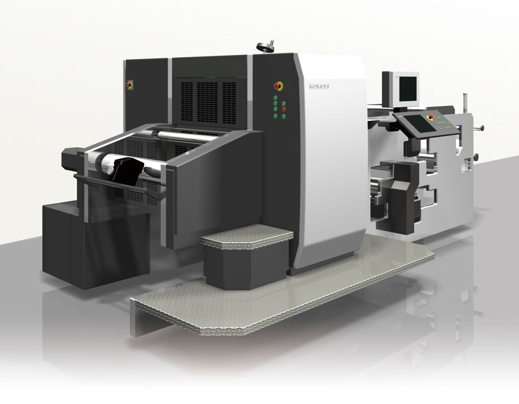
Left: Flatbed gravure offset printing press for fine lines PEPIO F20
Right: Roll-to-roll gravure offset printing press for fine lines PEPIO R20
Seria Group's expansion into the field of semiconductors
The Seria Group excels in providing screen printing and gravure offset printing technologies. As the automotive industry moves toward EVs and automated driving, and as companies adopt digital transformations, telecom infrastructure such as 5G, and expand data centers due to AI, the semiconductor industry's relevance is surging. Traditionally, semiconductor packages involved a single chip per package, but this method has limited design flexibility and yield. The emerging trend toward chiplets, which involves mounting multiple chips in a single package, is a response to these limitations.
Seria has promoted key technologies to advance chiplets, notably solder ball mounting and through via hole filling for interlayer conduction in multilayer substrates.
The solder ball mounting technology, developed in collaboration with Athlete FA Corporation, a leading global manufacturer of ball mounters. The required flux printing diameter and pitch have already exceeded the limits of miniaturization and printing coordinate accuracy possible with screen printing. Utilizing gravure offset printing, this partnership has achieved a groundbreaking advancement: the world's first successful ball mounting with a diameter of f30 μm and a pitch of 60 μm, surpassing the limits of screen printing. This technique ensures a printing coordinate accuracy of ±5 μm or less.
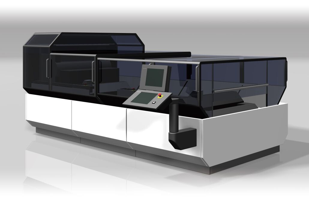
The through via hole filling technology employs a vacuum screen-printing machine, which prevents the introduction of voids (air bubbles) by printing in a vacuum. Avoiding voids is crucial, as they can expand and burst during thermal processing, compromising both reliability and yield. The SVM-6151IP, a semi-automatic vacuum coating machine equipped with CCD cameras, has been highly praised since its introduction. It has been adopted by numerous semiconductor-related companies worldwide. Furthermore, technological advancements such as the use of glass substrates and interposers for chiplet production are progressing. Looking ahead, Komori is committed to identifying opportunities in emerging sectors, improving production facilities, and developing technologies that align with contemporary needs, all in support of the semiconductor industry's growth.
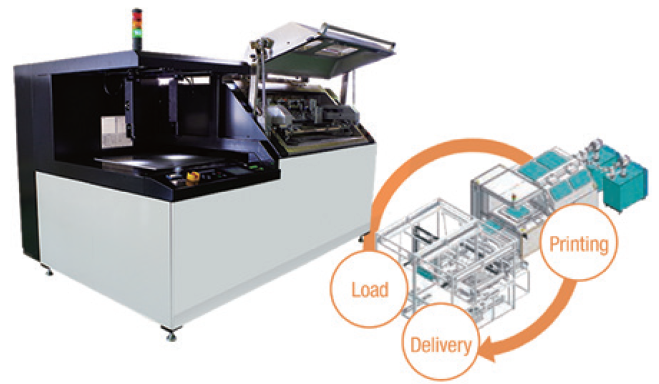
Vacuum coating machine SVM-6151IP automation proposal example